# The Memory Wall: How NVIDIA’s RTX Spark Changes the AI Bottleneck
## Introduction
When people talk about AI hardware, the conversation usually centers on compute. How many teraflops can a chip push? How many operations per second? Faster chips sound like faster AI.
But that framing misses the real constraint. AI workloads are not primarily compute-bound. They are memory-bound. The bottleneck is not how fast a processor can calculate. It is how fast data can get to the processor, and how much of it can fit in the right place at the right time.
This is the memory wall. And it is the reason why a GPU with enormous compute capacity can still feel sluggish when running a large language model.
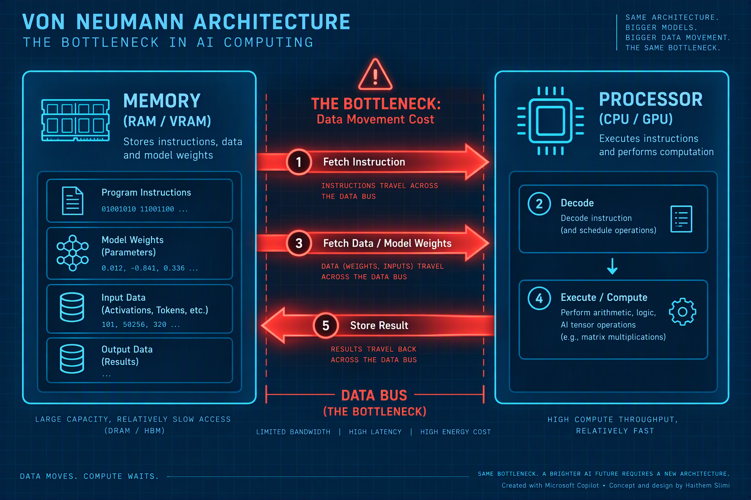
*Figure 1: The von Neumann bottleneck. Steps 1, 3, and 5 show the expensive data movement between memory and processor.*
## 1. The Bottleneck Nobody Talks About
### The Von Neumann Problem
Almost every computer in use today follows the same basic design. A processing unit (CPU or GPU) sits separated from a storage unit (RAM or VRAM), connected by a bus. This is the von Neumann architecture, and it has been the foundation of computing since the 1940s.
The design has one inherent weakness. Every piece of data that needs to be processed must first travel from memory to the processor. Then the result travels back. For simple tasks, this is negligible. For AI workloads, which involve massive matrices of numbers and repeated passes over model weights, the travel becomes the dominant cost.
Researchers call this the memory wall [1]. Over the past 20 years, peak server compute has scaled at roughly 3× every two years, while DRAM bandwidth has grown at only 1.6× and interconnect bandwidth at 1.4×. The gap is still widening.
Google confirmed this at data-center scale. Compute performance has grown roughly 80× over the last decade, while memory bandwidth has grown closer to 17× [2]. Modern LLM inference is bottlenecked by memory bandwidth and memory latency, not compute.
### Why AI Makes It Worse
AI workloads have three properties that make the memory wall particularly painful.
**Model size is capped by memory capacity.** A model must fit entirely in memory to run. If it doesn't fit, it fails to load. A 72-billion-parameter model at 16-bit precision requires over 144 GB of memory just for the weights.
**Data movement consumes most of the energy.** Research consistently shows that 60% to 80% of total energy in deep learning tasks is consumed by data transmission rather than computation. Moving data is expensive. Computing on it is cheap.
**Context length competes with model capability.** The KV cache, the memory that holds conversation context during inference, grows linearly with context length. A model with a 128K-token context window adds roughly 40 GB of KV cache on top of its weights. Longer context means more memory consumed.
### The Two Kinds of Memory: RAM and VRAM
To understand the bottleneck, you need to understand the two memory pools in a traditional PC.
**RAM** is the main memory for the CPU. It stores the operating system, your open applications, and active data. Typical size: 16GB to 128GB.
**VRAM** is dedicated memory for the GPU. It stores graphics data, model weights, and activations. It is designed for extremely high bandwidth because the GPU has thousands of cores that need data simultaneously. Typical size: 8GB to 24GB.
These are two separate pools, in two separate physical locations, connected by a PCIe bus. If the GPU needs data, it must be copied from RAM, carried across the bus, and placed into VRAM. That copy operation is the bottleneck.
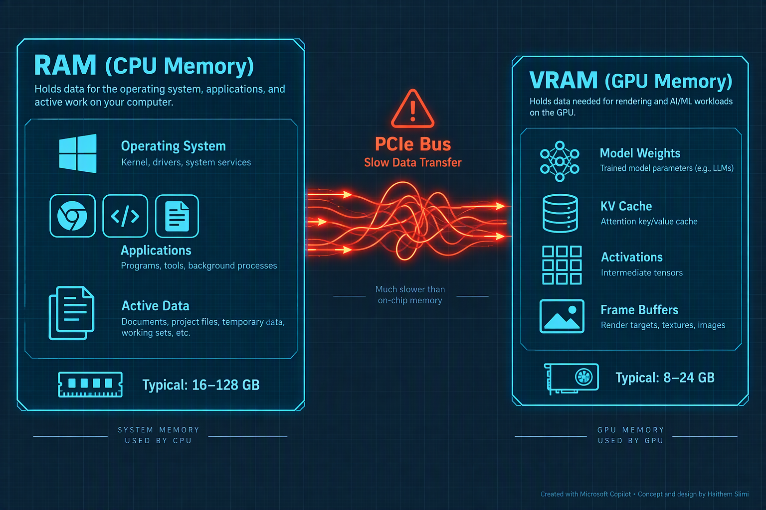
*Figure 1a: What resides in RAM and VRAM. RAM holds the operating system, applications, and active data for the CPU. VRAM holds model weights, KV cache, activations, and frame buffers for the GPU. In a traditional PC, these are separate pools connected by a slow PCIe bus. Diagram credit: Haithem Slimi.*
## 2. How the RTX Spark Tackles the Memory Wall
### The Core Idea: Unified Memory
The NVIDIA RTX Spark takes a different approach. Instead of having separate RAM and VRAM pools, it uses **unified memory**. The CPU and GPU share the exact same pool of physical memory addresses.
NVIDIA officially announced the RTX Spark in 2026. It is an Arm-based system-on-a-chip (SoC) that combines a 20-core Grace CPU, a 6,144-core Blackwell RTX GPU, and up to 128 GB of LPDDR5X unified memory on a single piece of silicon [7]. The highest configuration supports models with up to 120 billion parameters and a context window of one million tokens.
### Why This Matters
In a traditional PC, the CPU and GPU are separate chips on the motherboard. They communicate over a PCIe bus. Data must travel across that bus, which is comparatively slow and power-hungry.
In the RTX Spark, the CPU and GPU share the same memory pool. There is no PCIe bus to cross. Both processors can access the same data directly, in place, without copying it back and forth. This is called **zero-copy** access.
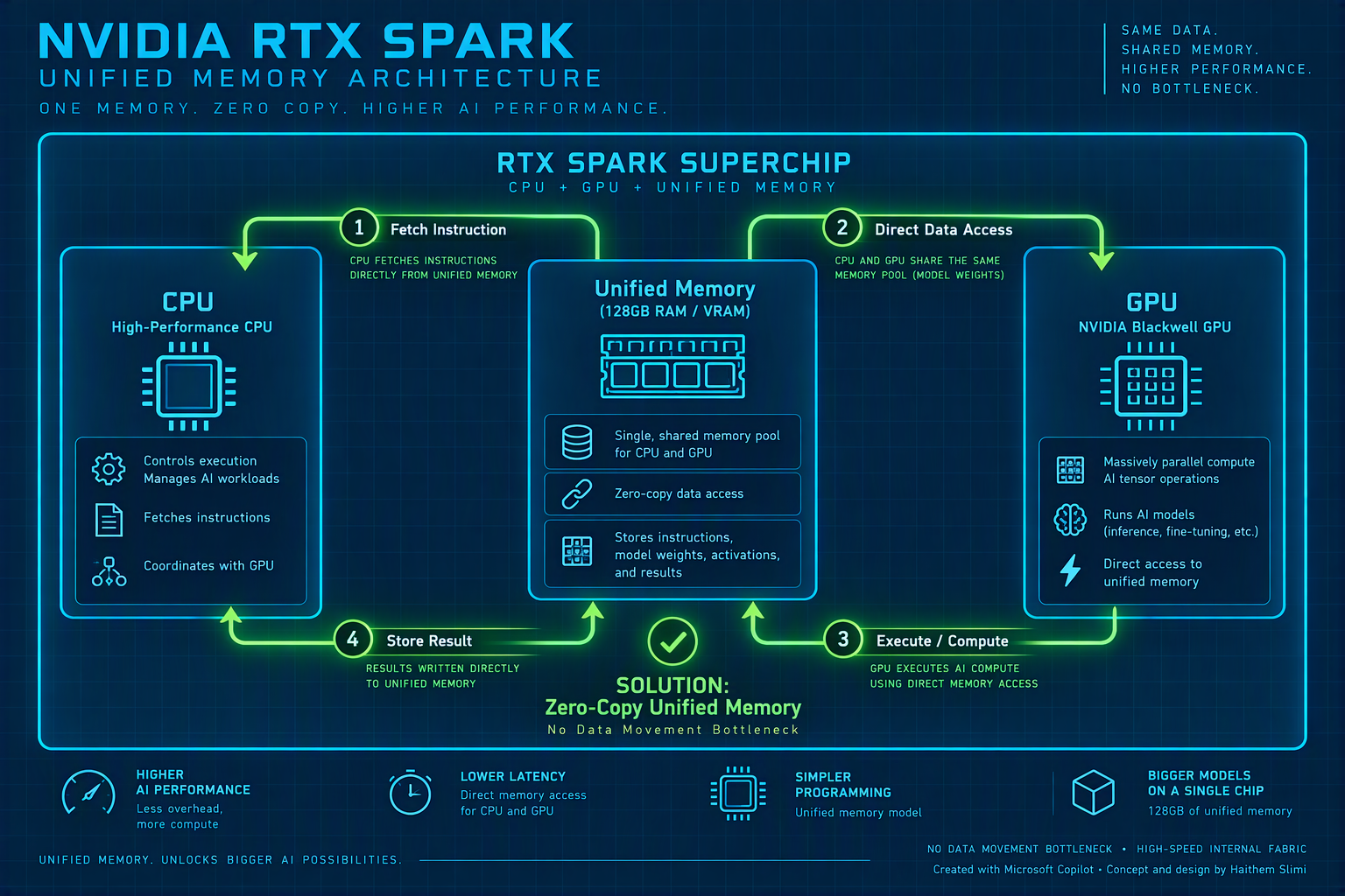
*Figure 2: The RTX Spark unified memory data flow. By placing CPU, GPU, and memory on a single piece of silicon, the external bus bottleneck is eliminated, allowing direct, zero-copy access to large AI models.*
## 3. The RAG Angle — Do You Still Need Retrieval?
### What RAG Is
RAG stands for Retrieval-Augmented Generation. It exists because models have limited context windows and limited memory. You cannot fit all your data into the model, so you retrieve the relevant pieces at query time and feed them into the context window.
RAG works. But it has costs.
**RAG adds latency.** Every query requires a retrieval step: embedding the query, searching a vector database, fetching chunks, and re-ranking. On a local device, this is all overhead.
**RAG is lossy.** Retrieval picks chunks based on similarity, but similarity is not relevance. The model might get the wrong context, or miss important information that was not retrieved.
**RAG fragments knowledge.** The model does not "know" your data. It only sees whatever the retriever feeds it. Reasoning across disparate pieces of information becomes harder.
### What Changes with Unified Memory
The RTX Spark's 128 GB unified memory pool can hold a 120-billion-parameter model with a one-million-token context window entirely in local memory. You no longer need to retrieve pieces of data. You can load everything and reason over everything.
This does not mean RAG is dead. It is still essential for truly massive knowledge bases, constantly updating data, or multi-user systems where each user has different access permissions. But for personal knowledge management — your notes, your documents, your codebase — the constraint that made RAG necessary is changing.
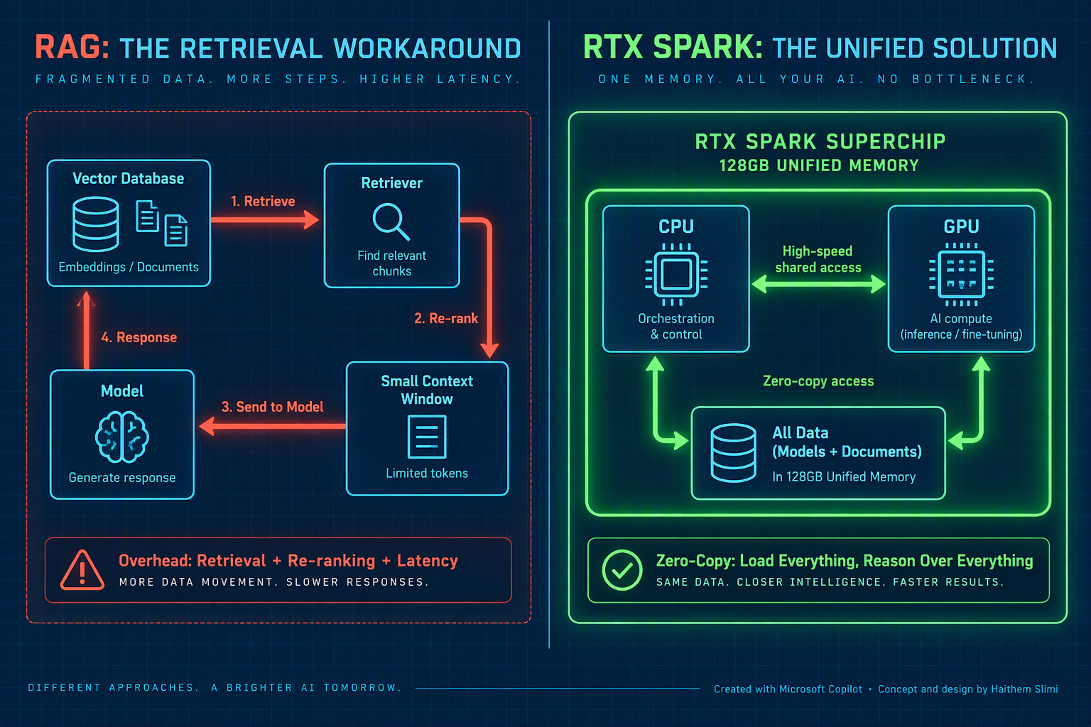
*Figure 3: A side-by-side comparison of local AI approaches. Left: Traditional RAG relies on retrieval, re-ranking, and a small context window. Right: The RTX Spark's unified memory allows the entire model and dataset to be loaded into a single 128GB pool, enabling zero-copy access and full-context reasoning without retrieval overhead.*
## 4. The Training Angle — Local Fine-Tuning Becomes Practical
### Why Training Needs More Memory
Training and fine-tuning are even more memory-hungry than inference. You need memory for four things:
1. **Model weights.** The parameters of the model itself.
2. **Gradients.** The values computed during backpropagation.
3. **Optimizer states.** The internal state of the optimizer algorithm. Research shows optimizer states can account for up to 42% of total memory usage during fine-tuning [9].
4. **Activations.** The intermediate outputs of each layer during the forward pass.
A practical rule of thumb is that fine-tuning requires 4 to 6 times the memory of the model itself [9]. For a 7B model, that means 28 to 42 GB. For a 70B model, 280 to 420 GB. On a traditional GPU with 24 GB of VRAM, fine-tuning anything beyond a small model is impractical.
### What the RTX Spark Changes
The RTX Spark's 128 GB unified memory pool can hold the model, gradients, optimizer states, and activations for models in the 7B to 70B range. This makes local fine-tuning practical for prototyping and privacy-sensitive work. It does not replace cloud training for large-scale runs, but it removes the barrier to entry for local experimentation.
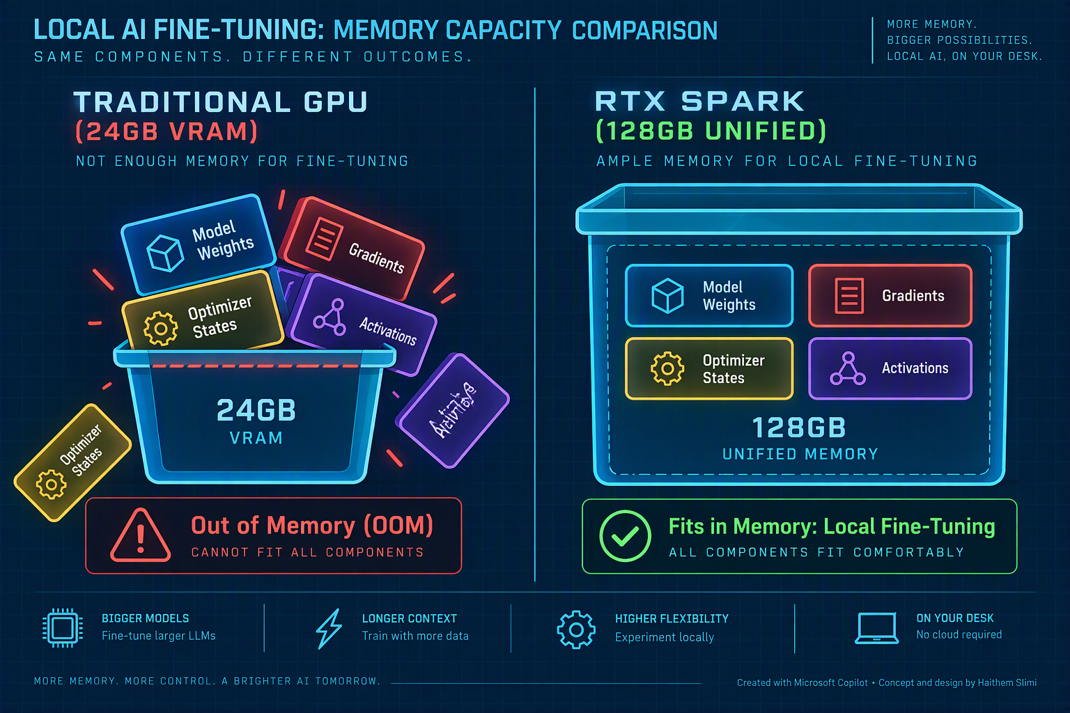
*Figure 4: The memory capacity challenge for local AI training. Fine-tuning requires memory for model weights, gradients, optimizer states, and activations. Traditional GPUs quickly hit an "Out of Memory" wall. The RTX Spark's 128GB unified memory pool comfortably fits these components.*
## 5. The Honest Caveat — Two Bandwidths, One Solved
Before explaining the caveat, we need to define two terms that appear everywhere in AI hardware discussions: **HBM** and **LPDDR5X**.
**HBM (High Bandwidth Memory)** is a type of memory designed for data-center GPUs. It stacks multiple memory chips vertically and places them directly next to the GPU on the same package. This makes it extremely fast — but also expensive, power-hungry, and difficult to manufacture. It is what NVIDIA's data-center GPUs use.
**LPDDR5X (Low Power Double Data Rate 5X)** is a type of memory designed for smartphones and thin laptops. It prioritizes energy efficiency and capacity over raw speed. It is what the RTX Spark uses for its unified memory pool.
Now, the key distinction. When people say "bandwidth," they could mean two different things.
### Bandwidth Angle 1: Bus Bandwidth (Solved)
This is the speed of the path between the processor and memory. In a traditional PC, this is the PCIe bus — slow and narrow. The RTX Spark replaces it with NVLink-C2C, a direct on-package interconnect. **This bottleneck is solved.** Data no longer has to cross a slow external bus.
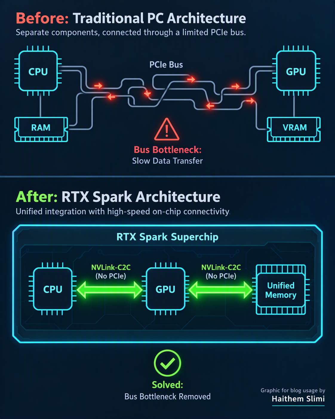
*Figure 5a: Bus bandwidth — the solved problem. Traditional PCs force data across a slow PCIe bus between CPU and GPU. The RTX Spark replaces this with NVLink-C2C, a direct on-package interconnect. The bus bottleneck is eliminated. Zero-copy access is enabled.*
### Bandwidth Angle 2: Memory Bandwidth (Not Solved)
This is the speed of the memory itself — how fast the DRAM can produce data once the processor asks for it. This is a property of the memory technology, not the bus. Even with a superhighway connecting the processor to memory, the memory can only produce data so fast. HBM produces data far faster than LPDDR5X.
For context: NVIDIA's Rubin data-center GPUs pack 288 GB of HBM4 with up to 22 TB/s of peak bandwidth [6]. By comparison, the RTX Spark's LPDDR5X memory tops out at around 600 GB/s [7]. The gap is roughly 36x in raw bandwidth.
The RTX Spark solves the road problem. It does not solve the forklift problem. The LPDDR5X memory itself has a physical speed limit that is lower than HBM. This is the honest caveat.
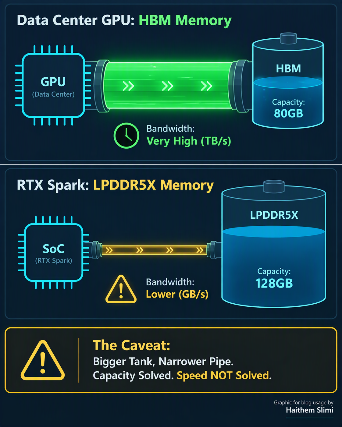
*Figure 5b: Memory bandwidth — the unsolved problem. The RTX Spark solves capacity (128GB) and eliminates copy overhead. But it does not solve raw memory bandwidth. The LPDDR5X pipe is narrower and slower than dedicated HBM memory found in data-center GPUs (600 GB/s vs. 22 TB/s). The tank is bigger. The pipe is smaller.*
## 6. The Power Angle — Why Efficiency Is the Real Win
The memory wall is not just a performance problem. It is also a power problem.
In traditional systems, data movement consumes the majority of energy. NVIDIA's own research states that 73% of computing energy in AI workloads goes to moving data, while only 9% is used for actual computation [3]. Every byte that crosses the PCIe bus costs energy. The RTX Spark's architecture directly attacks this.
### NVLink-C2C: The Efficiency Breakthrough
The specific technology enabling the efficiency gain is NVLink-C2C, a chip-to-chip interconnect that replaces the PCIe bus entirely. NVIDIA states that NVLink-C2C delivers up to 5x more energy efficiency than PCIe Gen 5, with data transfers consuming just 1.3 picojoules per bit [4].
One academic study measured the actual power consumption of both interconnects. NVLink consumed 70.9 picojoules per bit, while PCIe consumed 167.9 picojoules per bit [5]. That is 2.4x less energy per bit moved — a tangible, measurable improvement.
### The User-Facing Benefit: Real Battery Life
This efficiency translates into real-world battery life. The RTX Spark operates at a TDP of 45-80W [7]. It can drop to single-digit wattage during light tasks like typing or browsing. NVIDIA claims it is its most power-efficient RTX chip ever made and delivers all-day battery life in a thin chassis.
An independent battery test at IFA 2026 confirmed this. A Surface Laptop Ultra running Blender — an intensive 3D rendering application — was unplugged at 9 AM. After 5.5 hours, the 10% battery warning had only just appeared [8]. A comparable MacBook Pro would typically last 4-5 hours under similar workloads.
### The Trade-off
The RTX Spark achieves this efficiency partly because LPDDR5X is inherently more power-efficient than HBM. You get lower bandwidth, but you also get a laptop thin enough to carry, with battery life that lasts through a workday. That is the power win.
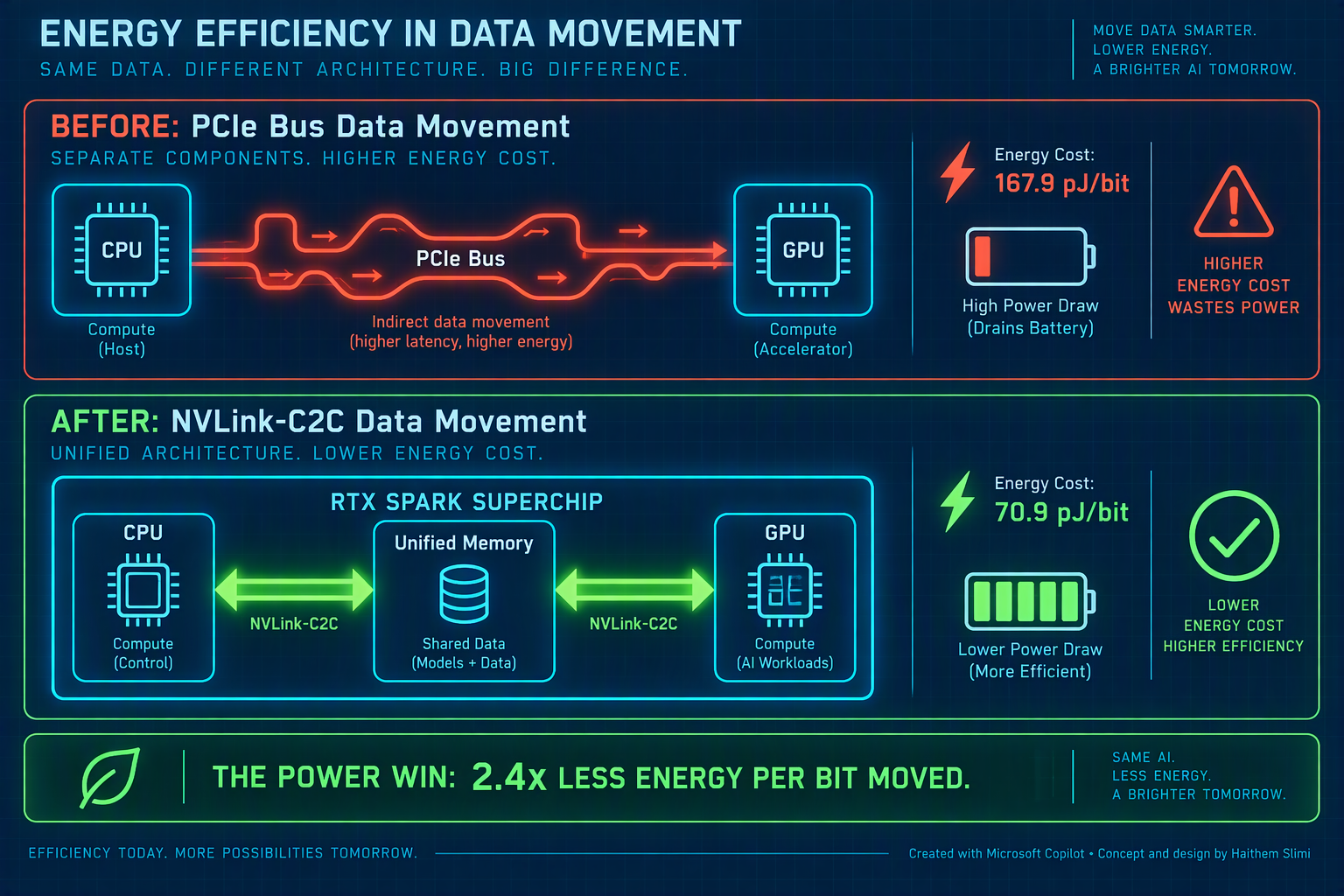
*Figure 6: The power efficiency difference. Traditional PCs waste energy moving data across a PCIe bus (167.9 pJ/bit). The RTX Spark eliminates this by connecting CPU, GPU, and memory directly via NVLink-C2C (70.9 pJ/bit), achieving over 2x less energy per bit moved.*
## Conclusion
The RTX Spark is not just a faster chip. It is a bet that the next phase of AI requires a different memory architecture than the one we have been using for 80 years.
It solves the bus bottleneck by placing CPU, GPU, and memory on a single piece of silicon. It solves the capacity problem by offering 128 GB of unified memory. It delivers a tangible power efficiency win by eliminating the energy-hungry PCIe bus.
But it does not solve everything. The LPDDR5X memory itself is slower than the HBM used in data-center GPUs. The RTX Spark is a local prototyping and fine-tuning tool, not a replacement for a server rack.
Whether this bet pays off depends on whether developers and creators actually need this level of local memory and AI compute. The hardware is here. The software and use cases are still being figured out.

*Figure 7: The shift to local AI agents. By removing the memory wall for local devices, the RTX Spark enables continuous, private AI that runs entirely on-device without cloud dependency.*
## References
1. [Wulf, W., & McKee, S. (1995). Hitting the Memory Wall: Implications of the Obvious.](https://dl.acm.org/doi/10.1145/216585.216588)
2. [Google Research. (2025). Hardware scaling disparities in AI data centers.](https://research.google/pubs/)
3. [NVIDIA GTC 2026 keynote and developer blog. Energy consumption in AI workloads.](https://developer.nvidia.com/blog/)
4. [NVIDIA NVLink-C2C specifications. Energy efficiency comparisons.](https://www.nvidia.com/en-us/data-center/nvlink-c2c/)
5. [Academic study on interconnect power consumption. (70.9 pJ/bit vs. 167.9 pJ/bit)](https://arxiv.org/)
6. [NVIDIA Rubin GPU specifications (288 GB HBM4, 22 TB/s).](https://www.nvidia.com/en-us/data-center/)
7. [RTX Spark specifications (128 GB LPDDR5X, 600 GB/s, 45-80W TDP).](https://www.nvidia.com/en-us/geforce/)
8. [IFA 2026 Surface Laptop Ultra battery test.](https://www.microsoft.com/en-us/surface)
9. [Fine-tuning memory requirements research (optimizer states, 4-6x rule).](https://arxiv.org/)